4.6 Molecular beam epitaxy
References
Molecular beam epitaxy (MBE) is a sophisticated technique used in the growth of semiconductor layers, structures and devices. It is a technique that is of immense importance to both the industrial and academic sectors. Those of you who take the Semiconductor Physics and Devices optional module next semester will learn how MBE is used for device fabrication.
In this section I will cover MBE from the point of view of fundamental surface processes. In particular, I'll briefly show how the topics we have discussed in this section of the module – adsorption, diffusion and thin film growth – underlie our understanding of MBE and thus our ability to fabricate sophisticated semiconductor structures. (Note that MBE is a suggested article topic).
MBE allows the controlled growth of semiconductor layers with monolayer precision. A simple schematic of a typical MBE system is shown in Prutton, Fig. 6.18. The layers are grown, as you should expect by now, under UHV conditions. Knudsen cells are used to deposit the various materials (eg Ga, As, In, Al etc…) onto a heated substrate which is rotated during growth to maximise growth homogeneity.
Shutters are used to switch the molecular beams on and off and an ion gauge, as described in Section 3.4, monitors the pressure. The MBE growth chamber will typically be coupled, via a valve, to an analysis chamber where electron or optical spectroscopies or STM may be carried out. A very important in situ diagnostic tool used to monitor the film quality during growth is reflection high energy electron diffraction (RHEED) (the electron gun and, as for LEED, fluorescent screen used to monitor diffraction patterns are shown in Fig. 6.18 of Prutton). We'll return to a discussion of this technique and its importance in MBE growth in Section 6.
To date, most MBE growth has involved III-V compounds (GaAs, InAs, AlGaAs, InSb etc…) although there is increasing interest in MBE-grown Si and SiGe structures. While MBE homoepitaxial growth processes (eg GaAs on GaAs, InAs on InAs etc..) are certainly very important, a wealth of fascinating physics has arisen from our ability to produce high quality semiconductor heterostructures using MBE.
For example, the band gap of the AlGaAs compound varies with the relative concentrations of Al and Ga – concentrations which are directly controllable in MBE. The ability to both control the band gap of a material via changes in its composition ( band gap engineering) and to epitaxially grow one layer of semiconductor on another revolutionised semiconductor fabrication processes and has led to the development of numerous important electronic and optoelectronic devices.
(If you're interested in this topic, next semester's Semiconductor Physics & Devices module discusses some of those devices in detail).
 Let's discuss some of the fundamental principles underlying MBE on the basis of the adsorption, diffusion and growth processes covered in the previous sections.
Until very recently MBE focussed on the growth of lattice-matched materials such as AlGaAs on GaAs which exhibit a layer-by-layer (FM) growth mode.
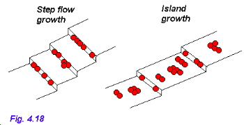
Layer-by-layer growth in MBE may proceed via two very distinct limiting mechanisms, related to the magnitude of the diffusion constant D (Fig. 4.18):
- D is such that the diffusion length << the average terrace width (the
distance between atomic
steps): growth occurs via the nucleation of islands on the terraces;
- D is such that the diffusion length >> the average terrace width;
adsorbed atoms can diffuse to step
edges where they attach. New terraces then "grow out" from the step edges at a rate dependent on the step density and growth rate. This is called step-flow growth.
As we'll see in Section 6, RHEED provides a method of distinguishing between these two growth mechanisms.
 The step
flow growth mechanism exhibits a considerable degree of anisotropy on GaAs(100) surfaces. Can you suggest some possible origins for this anisotropy?
Self-assembled quantum dots
 Very recently, there has been intense interest by a large number of research groups in the use of MBE to generate ultra-small islands (quantum dots) of semiconductor material. We'll discuss the electronic properties and synthesis of these structures in some detail in Section 8. For now, to finish this section of the module, try answering the following question.
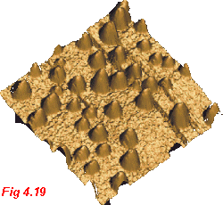
 An STM image
of InAs islands grown by MBE on a GaAs substrate is shown in Fig 4.19. Give reasons why InAs, unlike AlGaAs or AlAs, for example, forms nanoscale dots on the GaAs substrate.
Home
 Let's discuss some of the fundamental principles underlying MBE on the basis of the adsorption, diffusion and growth processes covered in the previous sections.
Until very recently MBE focussed on the growth of lattice-matched materials such as AlGaAs on GaAs which exhibit a layer-by-layer (FM) growth mode.
Layer-by-layer growth in MBE may proceed via two very distinct limiting mechanisms, related to the magnitude of the diffusion constant D (Fig. 4.18):

 Very recently, there has been intense interest by a large number of research groups in the use of MBE to generate ultra-small islands (quantum dots) of semiconductor material. We'll discuss the electronic properties and synthesis of these structures in some detail in Section 8. For now, to finish this section of the module, try answering the following question.