
In Wood’s notation, if the surface reconstruction or adsorbed overlayer has primitive translation vectors of length:

 degrees wrt to the substrate unit cell, the structure is referred to as:

 is omitted.
So, the  reconstruction of the Si(100) surface described in section 2.3, in Wood’s notation becomes:
 An STM image of the Si(100)(2x1) surface is shown to the
right. The dimer rows are clearly visible.
 Q. What is the separation of the Si(100) dimer rows in the STM image given that the bulk lattice constant of Si is 0.543 nm?
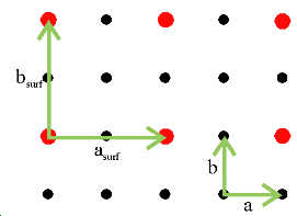
Fig.2.5 (a)
fcc(100)( x
x  )R45o or fcc(100)c(2x2)
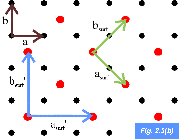 The surface structure shown in Fig. 2.5(b) may be termed a (
 x
x  ) R45o reconstruction with basis vectors asurf and bsurf. However, it is also common for this structure to be referred to as a c(2x2) structure where the c stands for centred.
That is, instead of considering the surface lattice vectors as rotated by 45o from the substrate vectors, a different unit cell may be defined by the basis vectors asurf’ and bsurf’ which are aligned with the substrate basis vectors. In this case the unit cell has an atom at its centre.
It is very important to note that the centred notation, although very commonly used, does not represent a primitive unit cell. To distinguish a c(2x2) structure from a true primitive (2x2) unit cell (as shown in Fig. 2.5(a)) we add the letter "p" (for primitive). So, the structure shown in Fig. 2.5 (a) is commonly referred to as a p(2x2) reconstruction.
 Now try sketching an
example of a (i) fcc(110)(2x1); (ii) fcc(111)(2x1) and
(iii) fcc(111)( x
x  )R30o superstructure.
Si(111)(7x7)
The most complex reconstruction of a clean semiconductor surface is the (7x7) reconstruction of Si(111). This remarkable structure forms when a Si(111) sample is heated at temperatures above ~ 900oC in ultra high vacuum (UHV).
 We will discuss UHV techniques and technology in section 3 but for now why do you think very high vacuums are needed to study surfaces?
It took approximately 30 years and the efforts of a very large number of surface theorists and experimentalists to determine the atomic structure of the (7x7) surface.
Both electron diffraction (discussed in section 2.5) and STM (Section 7) were instrumental in elucidating the structural properties of the (7x7) surface.
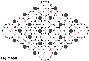 To get some idea of its complexity, and thus just why it took 30 years to "work out" the structure
compare the model of the the (7x7) unit cell shown in Fig. 2.6(a) with the ideal bulk terminated Si(111) surface unit cell (i.e. a (1x1) structure) (Fig. 2.6(b)). In Fig. 2.6(a) the large black circles represent the first layer atoms, the smaller black circles the second layer atoms, the grey circles the third layer and the smallest circles (dots!) represent the fourth layer atoms which correspond to bulk atoms
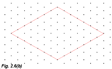 For comparison, only the top layer atoms of the ideal, bulk-like (1x1) termination are shown in Fig. 2.6(b).
DO NOT for now worry about the details of the (7x7) structure - just try to appreciate the huge amount of surface rearrangement (over three atomic layers) that is necessary to produce it!
The important fact to remember is that the (7x7) surface has a lower free energy than the "ideal" (1x1) surface. There are 19 dangling bonds in the (7x7) unit cell compared with 49 in the equivalent surface area on the (1x1) surface - a considerable reduction in dangling bond density.
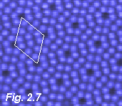
An STM image of the (7x7) surface is shown in Fig. 2.7. The unit cell is marked and the individual atoms of the topmost layer (the adatoms) are visible in each triangular half of the unit cell. These atoms correspond to the largest filled circles in the model shown in Fig. 2.6(a).
The history, physics and chemistry of the Si(111)(7x7) structure is a suggested "article" topic.
GaAs(110)(1x1)
Semiconductor surfaces are not all quite as complex as Si(111)(7x7)!
GaAs(110) is an example of a semiconductor surface that relaxes but does not reconstruct.
GaAs is a compound or polar semiconductor - due to the electronegativity difference between Ga and As the interatomic bonds in the compound are not purely covalent but have some ionic character. As we’ll see in Section 4, this has important implications regarding the properties of a polar semiconductor surface.
A very nice schematic drawing of the GaAs(110) surface can be found at K. Hermann's web site . (You'll need to scroll down the page a little to see the drawing (it's #3)). The GaAs(110) surface is also illustrated in Fig. 3.37 of Prutton, Fig. 3.5 of Luth and Fig. 4.43 of Zangwill. The surface relaxes via the Ga atom moving towards the surface and the As atom moving away from the surface. This structural modification is accompanied by an electronic modification at the surface - electronic charge is transferred from the Ga to the As atom. The close relationship between the structural and electronic properties of semiconductor surfaces is something we will return to in Section 4.