Transmission Electron Microscopy (TEM)
See down the the scale of molecules and atoms with TEM
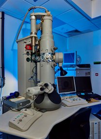
TEM at a glance
TEM is a microscopy technique capable of providing very high resolution images down to a level of several Angstroms (~ 0.19nm). It images thin (100s nms) samples via the interaction of electrons as they pass through a specimen. Detecting a range of resultant secondary signals allows for the study of nano-scale morphological and chemical features of materials down to near atomic levels.
Applications
- Bright field imaging
- Electron diffraction
- Dark field imaging
- Energy Dispersive X-ray Spectroscopy (EDS)
- Electron Energy Loss Spectroscopy (EELS)
- Scanning Transmission Electron Spectroscopy (STEM)
- Nanotomography (3D profiling)
Images Courtesy of Vladimir Korolkov Photography and Lubrizol Ltd.
How does TEM work?
An electron source at the top of the microscope emits electrons that travel through a vacuum in the column of the microscope. Electromagnetic lenses are used to focus the electrons into a very thin beam and this is then directed through the specimen of interest. The electrons passing through the specimen then impact on a detector. Traditional bright field imaging relies on incident electrons being scattered and disappearing from the beam depending upon the compositional density and crystal orientation of the sample. The intensity of un-scattered electrons gives rise to a "shadow image" of the specimen, with different parts of a specimen displayed in varied darkness according to density. By rotating a sample, and taking multiple images at each rotation, it is also possible to build a 3D representation of the specimen (tomography).
The crystal structure of samples with regular atomic structure (crystalline material) may also be analysed via electron diffraction. Positive interference in the back focal plane leads to discreet spots of electron localisation, which can then be visualised by mapping the back focal plane to the imaging apparatus. The diffraction patterns can then be used to analyse to the crystal structure of the specimen.
X-ray emission consequent to the interaction of the primary electron beam with the sample, can also be detected by an energy-dispersive spectrometer (EDS) within the TEM. As the resulting X-ray energies are characteristic of the atomic structure of the element they originated from, the spectra generated can be used to identify the constituent elements.
It is also possible to measure the loss of energy from the inelastic scattering of electrons in specimen transmission (EELS). This information can be used to infer elemental composition, chemical bonding, valence and conduction band electronic properties.
Our TEM facilities
Hosted at the Nanoscale and Microscale Research Centre (nmRC).
-
-
Field emission electron gun (FEG) instrument, providing a high brightness and high stability electron source for use at 100kV and 200kV.
-
A point resolution of 0.19nm allows the ultrahigh resolution analysis of materials, on the nanometer scale.
-
Bright Field STEM Detector.
-
High Angle Annular Dark Field (HAADF) STEM Detector.
-
Gatan K3 IS camera. This is a 23.6 megapixel, electron counting direct detection (DDE) camera. Capable of 150 frames per second at full view, or >3500fps at 256x256 pixels.
-
Gatan Tridiem Filter Spectrometer and 2K x 2K CCD camera, configured for use at 100kV and 200kV. Enables elemental mapping via Electron Energy Loss Spectroscopy (EELS) and Energy Filtered TEM (EFTEM).
-
Oxford Instruments 80mm X-Max system for energy dispersive x-ray spectroscopy (EDS) analysis.
-
Room Temperature Tomograpghy: Gatan 916 Room temp tomography holder with up to 80 degrees tilt. Allows tilt series acquisition to generate 3D images.
-
Cryo-tomography and cryo transfer: Gatan 914 & Gatan Elsa Cryo-tomography holders including cold controller/ cryo-workstation.
-
Electrical holder. Gatan 936 DT analytical LN2 holder with temperature controller with EBIC stage option (4 electrical connections) plus Smart EBIC. Allows the electrical properties of samples to be related to the microstructure - e.g., defects in semiconductors.
-
Gatan 4004 heating and gas exchange holder. Allows samples to be heated up to 800 oC, or air sensitive sample analysis.
-
LaB6 TEM for high throughput, high versatility analysis at 80kV or 200kV.
-
Gatan OneView camera. High resolution, 16-megapixel CMOS camera for both low and high dose applications. Capable of 25 full frames per second or 300fps at 512x512 pixels.
-
Bright field STEM detector
-
Oxford Instruments X-MaxN 80 TLE EDS detector for chemical analysis.
-
Gatan Enfinium EELS detector
-
HADDF detector
-
Range of specialised sample rods including heating and cryogenic stages for variable temperature work and an analytical stage for tomographic and high contrast chemical analysis.
-
MEMS Heating holder. DENSsolutions Wildfire S3 capable of analyses up to 1300oC with millisecond heat and quench speed, and nanoscale sample drift with step changes of hundreds of degrees. Enables EELS and EDS mapping at elevated temperatures.
FEI Tecnai G12 12 Biotwin
-
Tomography compustage for tomographic characterisation
-
Cryo-stage for low temperature observation of temperature dependent or hydrated samples
-
Ideal for low-contrast, beam-sensitive biological specimens, or other soft materials such as polymers.
Publications of Interest
- Characterisation of soot in oil from a gasoline direct injection engine using Transmission Electron Microscopy, la Rocca, A., Bonatesta, F., Fay, M. W. & Campanella, F., Tribology International,86, 77–84 (2015).
- Additive manufacture of complex 3D Au-containing nanocomposites by simultaneous two-photon polymerisation and photoreduction, Hu, Q., Sun, X.-Z., Parmenter, C. D. J., Fay, M. W., Smith, E. F., Rance, G. A., He, Y., Zhang, F., Liu, Y., Irvine, D., Tuck, C., Hague, R. & Wildman, R., Scientific Reports,7, 17150 (2017).
- A one-pot-one-reactant synthesis of platinum compounds at the nanoscale, Stoppiello, C. T., Biskupek, J., Li, Z. Y., Rance, G. A., Botos, A., Fogarty, R. M., Bourne, R. A., Yuan, J., Lovelock, K. R. J., Thompson, P., Fay, M. W., Kaiser, U., Chamberlain, T. W. & Khlobystov, A. N. Nanoscale,9, 14385–14394 (2017).
- Synthesis of hydroxylated group IV metal oxides inside hollow graphitised carbon nanofibers: nano-sponges and nanoreactors for enhanced decontamination of organophosphates, Astle, M. A., Rance, G. A., Fay, M. W., Notman, S., Sambrook, M. R. & Khlobystov, A. N., Journal of Materials Chemistry A,6, 20444–20453 (2018).
- Formation of hollow carbon nanoshells from thiol stabilised silver nanoparticles via heat treatment, Watts, J. A., Fay, M. W., Rance, G. A., Brown, P. D. & Khlobystov, A. N., Carbon, 139, 538–544 (2018).
- Asymmetric Hybrid Polyoxometalates: A Platform for Multifunctional Redox-Active Nanomaterials, Hampson, E., Cameron, J. M., Amin, S., Kyo, J., Watts, J. A., Oshio, H. & Newton, G. N., Angewandte Chemie International Edition,58, 18281–18285 (2019).
- Bond Dissociation and Reactivity of HF and H2O in a Nano Test Tube, Biskupek, J., Skowron, S. T., Stoppiello, C. T., Rance, G. A., Alom, S., Fung, K. L. Y., Whitby, R. J., Levitt, M. H., Ramasse, Q. M., Kaiser, U., Besley, E. & Khlobystov, A. N., ACS Nano,14, 11178–11189 (2020).
- Quantifying soot nanostructures: Importance of image processing parameters for lattice fringe analysis, Pfau, S. A., la Rocca, A. & Fay, M. W., Combustion and Flame,211, 430–444 (2020).
- Using microfluidics for scalable manufacturing of nanomedicines from bench to GMP: A case study using protein-loaded liposomes, Webb, C., Forbes, N., Roces, C. B., Anderluzzi, G., Lou, G., Abraham, S., Ingalls, L., Marshall, K., Leaver, T. J., Watts, J. A., Aylott, J. W. & Perrie, Y., International Journal of Pharmaceutics, 582, 119266 (2020).
- Cryo-FIB-lift-out: practically impossible to practical reality, Parmenter C. D. & Nizamudeen, Z. A., Journal of Microscopy,281, 157–174 (2021).